


 Marcy's Musings: The Growing Industry
 It’s Only Common Sense: Here’s What To Do After IPC APEX EXPO 2024
 Dan’s Biz Bookshelf: Seeing the How
Sweeping Lasers Snap Together Nanoscale Geometric Grids
June 24, 2015 | Brookhaven National LaboratoryEstimated reading time: 3 minutes
Down at the nanoscale, where objects span just billionths of a meter, the size and shape of a material can often have surprising and powerful electronic and optical effects. Building larger materials that retain subtle nanoscale features is an ongoing challenge that shapes countless emerging technologies.
Now, scientists at the U.S. Department of Energy's Brookhaven National Laboratory have developed a new technique to rapidly create nano-structured grids for functional materials with unprecedented versatility.
"We can fabricate multi-layer grids composed of different materials in virtually any geometric configuration," said study coauthor and Brookhaven Lab scientist Kevin Yager. "By quickly and independently controlling the nanoscale structure and the composition, we can tailor the performance of these materials. Crucially, the process can be easily adapted for large-scale applications."
The results—published online June 23 in the journal Nature Communications—could transform the manufacture of high-tech coatings for anti-reflective surfaces, improved solar cells, and touchscreen electronics.
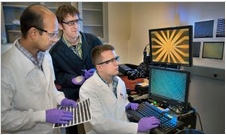
The scientists synthesized the materials at Brookhaven Lab's Center for Functional Nanomaterials(CFN) and characterized the nanoscale architectures using electron microscopy at CFN and x-ray scattering at the National Synchrotron Light Source—both DOE Office of Science User Facilities.
The new technique relies on polymer self-assembly, where molecules are designed to spontaneously assemble into desired structures. Self-assembly requires a burst of heat to make the molecules snap into the proper configurations. Here, an intensely hot laser swept across the sample to transform disordered polymer blocks into precise arrangements in just seconds.
"Self-assembled structures tend to automatically follow molecular preferences, making custom architectures challenging," said lead author Pawel Majewski, a postdoctoral researcher at Brookhaven. "Our laser technique forces the materials to assemble in a particular way. We can then build structures layer-by-layer, constructing lattices composed of squares, rhombuses, triangles, and other shapes."
For the first step in grid construction, the team took advantage of their recent invention of laser zone annealing (LZA) to produce the extremely localized thermal spikes needed to drive ultra-fast self-assembly.
To further exploit the power and precision of LZA, the researchers applied a heat-sensitive elastic coating on top of the unassembled polymer film. The sweeping laser's heat causes the elastic layer to expand—like shrink-wrap in reverse—which pulls and aligns the rapidly forming nanoscale cylinders.
"The end result is that in less than one second, we can create highly aligned batches of nano-cylinders," said study coauthor Charles Black, who leads the Electronic Nanomaterials group at CFN. "This order persists over macroscopic areas and would be difficult to achieve with any other method."
To make these two-dimensional grids functional, the scientists converted the polymer base into other materials.
One method involved taking the nano-cylinder layer and dipping it into a solution containing metal salts. These molecules then glom onto the self-assembled polymer, converting it into a metallic mesh. A wide range of reactive or conductive metals can be used, including platinum, gold, and palladium.
They also used a technique called vapor deposition, where a vaporized material infiltrates the polymer nano-cylinders and transforms them into functional nano-wires.
Layer-by-layer lattice
The first completed nano-wire array acts as the foundation of the full lattice. Additional layers, each one following variations on that same process, are then stacked to produce customized, crisscrossing configurations—like chain-link fences 10,000 times thinner than a human hair.
"The direction of the laser sweeping across each unassembled layer determines the orientation of the nano-wire rows," Yager said. "We shift that laser direction on each layer, and the way the rows intersect and overlap shapes the grid. We then apply the functional materials after each layer forms. It's an exceptionally fast and simple way to produce such precise configurations."
Study coauthor Atikur Rahman, a CFN postdoctoral researcher, added, "We can stack metals on insulators, too, embedding different functional properties and interactions within one lattice structure.
"The size and the composition of the mesh make a huge difference," Rahman continued. "For example, a single layer of platinum nano-wires conducts electricity in only one direction, but a two-layer mesh conducts uniformly in all directions."
LZA is precise and powerful enough to overcome interface interactions, allowing it to drive polymer self-assembly even on top of complex underlying layers. This versatility enables the use of a wide variety of materials in different nanoscale configurations.
"We can generate nearly any two-dimensional lattice shape, and thus have a lot of freedom in fabricating multi-component nanostructures," Yager said. "It's hard to anticipate all the technologies this rapid and versatile technique will allow."
Brookhaven National Laboratory is supported by the Office of Science of the U.S. Department of Energy. The Office of Science is the single largest supporter of basic research in the physical sciences in the United States, and is working to address some of the most pressing challenges of our time. For more information, please visit science.energy.gov.
Share on:


Suggested Items
Groundbreaking Ceremony Marks the Beginning of a New Era for Newccess Industrial; The Construction of the MINGXIN Building
04/12/2024 | Newccess IndustrialOn a clear and sunny day in March, the groundbreaking ceremony for the MINGXIN Building took place in Shenzhen, China. This moment marked the official commencement of construction for a project that will reshape the semiconductor materials industry.
The Need for a Holistic Global Sustainability Standard
04/10/2024 | Michael Ford, Aegis SoftwareNo one can deny that the resources of our fragile planet are finite. The environment seems like a third party, subject to constant degradation. We’re acutely aware of the effects of pollution on our climate, and despite our “throw-away” culture, recycling and recovery of materials has remained relatively expensive, even as we use more energy just to survive.
iNEMI Publishes Four Roadmap Topics
04/04/2024 | iNEMIThe International Electronics Manufacturing Initiative (iNEMI) announces the availability of the first roadmap topics in the new iNEMI Roadmap format. Printed circuit boards, sustainable electronics, smart manufacturing, and mmWave materials and test are now available online.
Insulectro’s 'Storekeepers' Extend Their Welcome to Technology Village at IPC APEX EXPO
04/03/2024 | InsulectroInsulectro, the largest distributor of materials for use in the manufacture of PCBs and printed electronics, welcomes attendees to its TECHNOLOGY VILLAGE during this year’s IPC APEX EXPO at the Anaheim Convention Center, April 9-11, 2024.
Checking In With ICAPE Group
04/03/2024 | Nolan Johnson, I-Connect007ICAPE Group’s field application engineer Erik Pederson drills down on sustainability, supply chain resiliency, and what value engineering really looks like in this exclusive interview. Founded in 1999, European-based ICAPE Group provides 21 million printed circuit boards and over six million technical parts to manufacturers every month. With 30 PCB manufacturing partners globally and 50 partners providing a wide array of technical parts, ICAPE Group has operations in China, Taiwan, Thailand, South Korea, Vietnam, South Africa, Europe, Mexico, and the United States. The company also focuses on the value proposition for its customers.