


 Marcy's Musings: The Growing Industry
 It’s Only Common Sense: Here’s What To Do After IPC APEX EXPO 2024
 Dan’s Biz Bookshelf: Seeing the How
New Technique Enables 3D Mapping of Magnetic Patterns
July 8, 2015 | HZBEstimated reading time: 2 minutes
An international collaboration has succeeded in using synchrotron light to detect and record the complex 3D magnetisation in wound magnetic layers. This technique could be important in the development of devices that are highly sensitive to magnetic fields, such as in medical diagnostics for example. Their results are published now in Nature Communications.
3D structures in materials and biological samples can be investigated today using X-ray tomography. This is done by recording images layer-by-layer and assembling them on a computer into a three-dimensional mapping. But so far there has been no comparable technique for imaging 3D magnetic structures on nm length scales. Now teams from HZB and the Institut für Festkörperphysik / Technische Universität Dresden in collaboration with research partners from institutions in California (1) have developed a technique with which this is possible.
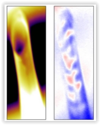
Mapping of rolled-up magnetic samples
They studied the magnetisation in rolled-up tubular magnetic nanomembranes (nickel or cobalt-palladium) about two layers thick. To obtain a 3D mapping of the magnetisation in the tubes, the samples were illuminated with circularly polarized X-rays. Using the X-ray microscope at the Advanced Light Source and the X-ray Photoemission Electron Microscopy (XPEEM) beamline at BESSY II, the samples were slightly rotated for each new image so that a series of 2D images was created. “The polarised light penetrated the magnetic layers from different angles. Using XPEEM, we were not only able to measure the magnetic features at the surface, but also obtained additional information from the “shadow”, explains Florian Kronast, who is responsible for the XPEEM beamline at HZB.
3D reconstruction of magnetic patterns
In the end, the physicists were successful in reconstructing the magnetic features on the computer in three dimensions.
“These samples displayed structures not smaller than 75 nanometres. But with this method we should be able to see even smaller structures and obtain a resolution of 20 nanometres”, explains Florian Kronast. However, so far only electron holography could be considered for mapping magnetic domains of three-dimensional objects at the nanometre scale. This required very complicated sample preparation and the magnetisation could only be indirectly determined through the resulting distribution of the magnetic field. “Our process enables you to map the magnetisation in directly in 3D. Knowledge of the magnetisation is prerequisite for improving the sensitivity of magnetic field detectors.”
Sensors for weak magnetic fields
The new method could be of interest to anyone involved with extremely small magnetic features within small volumes, such as those developing more sensitive devices for medical imaging, for example. Procedures like magnetoencephalography depend on externally detecting very weak magnetic fields created by the electrical activity of individual nerve cells – using appropriately sensitive detectors.
Share on:


Suggested Items
Inkjet Solder Mask ‘Has Arrived’
04/10/2024 | Pete Starkey, I-Connect007I was delighted to be invited to attend an interactive webinar entitled “Solder Mask Coating Made Easy with Additive Manufacturing,” hosted by SUSS MicroTec Netherlands in Eindhoven. The webinar was introduced and moderated by André Bodegom, managing director at Adeon Technologies, and the speakers were Mariana Van Dam, senior product manager PCB imaging solutions at AGFA in Belgium; Ashley Steers, sales manager at Electra Polymers in the UK; and Dr. Luca Gautero, product manager at SUSS MicroTec Netherlands.
NetVia Group Acquires Direct Imaging from Mivatek
04/09/2024 | Miva TechnologiesMiva Technologies is pleased to announce NetVia Group, Irving, TX has acquired a new Miva 2400NG Dual Tray Direct Imaging System with 30-micron capabilities for inner, outer and soldermask imaging.
Teledyne to Acquire Adimec
02/13/2024 | TeledyneTeledyne Technologies Incorporated announced that it has entered into an agreement to acquire Adimec Holding B.V. and its subsidiaries.
Real Time with... productronica 2023: MivaTek Global Advances Technology With High-res Imaging System
12/08/2023 | Real Time with...productronicaMivaTek's Brendan Hogan talks about how the company employs Digitally Adaptive Rasterization Technology (DART) in their high-res imaging equipment. He also shares how the blurred line between semiconductors and microelectronics is driving broader application of the imaging process.
Keysight Enables Validation of Arbe 4D Imaging Radar Chipset
11/30/2023 | Keysight Technologies, Inc.Keysight Technologies, Inc. announces that Arbe has selected the E8719A Radar Target Solution (RTS) to test the Arbe 4D imaging radar chipset for automotive applications.