


 Marcy's Musings: The Growing Industry
 It’s Only Common Sense: Here’s What To Do After IPC APEX EXPO 2024
 Dan’s Biz Bookshelf: Seeing the How
Visualizing Atoms of Perovskite Crystals
January 10, 2016 | Okinawa Institute of Science and Technology (OIST) Graduate UniversityEstimated reading time: 2 minutes
Organic-inorganic perovskite materials are key components of the new generation of solar cells. Understanding properties of these materials is important for improving lifetime and quality of solar cells. Researchers from the Energy Materials and Surface Sciences (EMSS) Unit, led by Prof. Yabing Qi, at the Okinawa Institute of Science and Technology Graduate University (OIST) in collaboration with Prof. Youyong Li's group from Soochow University (China) and Prof. Nam-Gyu Park's group from Sungkyunkwan University (Korea) report in the Journal of the American Chemical Society the first atomic resolution study of organic-inorganic perovskite.
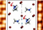
Perovskites are a class of materials with the general chemical formula ABX3. A and B are positive ions bound by negative ions X. Organic-inorganic perovskites used in solar cells are usually methylammonium lead halides (CH3NH3PbX3, where X is bromine, iodine, or chlorine). The OIST scientists used a single crystal of methylammonium lead bromide (CH3NH3PbBr3) to create topographic images of its surface with a scanning tunneling microscope.
This microscope uses a conducting tip that moves across the surface in a manner very similar to a finger moving across a Braille sign. While the bumps in Braille signs are a few millimetres apart, the microscope detects bumps that are more than million times smaller -- atoms and molecules. This is achieved by the quantum tunneling effect -- the ability of an electron to pass through a barrier. The probability of an electron passing between the material surface and the tip depends on the distance between the two. The resulting atomic-resolution topographic images reveal positions and orientations of atoms and molecules, and also provide a detailed look at structural defects in the surface.
"At room temperature atoms and molecules are quite mobile, so we decided to freeze the crystal to almost absolute zero (-269ºC) to get a good picture of its atomic structure," says Dr Robin Ohmann, a member of the EMSS Unit and the first author of the paper. The crystal was cut and studied in a vacuum to avoid contamination of the surface. Dr Ohmann's colleagues from Soochow University calculated atomic structures using principles of quantum physics and then compared them with scanning tunneling microscopy data.
Page 1 of 2
Share on:


Suggested Items
Groundbreaking Ceremony Marks the Beginning of a New Era for Newccess Industrial; The Construction of the MINGXIN Building
04/12/2024 | Newccess IndustrialOn a clear and sunny day in March, the groundbreaking ceremony for the MINGXIN Building took place in Shenzhen, China. This moment marked the official commencement of construction for a project that will reshape the semiconductor materials industry.
The Need for a Holistic Global Sustainability Standard
04/10/2024 | Michael Ford, Aegis SoftwareNo one can deny that the resources of our fragile planet are finite. The environment seems like a third party, subject to constant degradation. We’re acutely aware of the effects of pollution on our climate, and despite our “throw-away” culture, recycling and recovery of materials has remained relatively expensive, even as we use more energy just to survive.
iNEMI Publishes Four Roadmap Topics
04/04/2024 | iNEMIThe International Electronics Manufacturing Initiative (iNEMI) announces the availability of the first roadmap topics in the new iNEMI Roadmap format. Printed circuit boards, sustainable electronics, smart manufacturing, and mmWave materials and test are now available online.
Insulectro’s 'Storekeepers' Extend Their Welcome to Technology Village at IPC APEX EXPO
04/03/2024 | InsulectroInsulectro, the largest distributor of materials for use in the manufacture of PCBs and printed electronics, welcomes attendees to its TECHNOLOGY VILLAGE during this year’s IPC APEX EXPO at the Anaheim Convention Center, April 9-11, 2024.
Checking In With ICAPE Group
04/03/2024 | Nolan Johnson, I-Connect007ICAPE Group’s field application engineer Erik Pederson drills down on sustainability, supply chain resiliency, and what value engineering really looks like in this exclusive interview. Founded in 1999, European-based ICAPE Group provides 21 million printed circuit boards and over six million technical parts to manufacturers every month. With 30 PCB manufacturing partners globally and 50 partners providing a wide array of technical parts, ICAPE Group has operations in China, Taiwan, Thailand, South Korea, Vietnam, South Africa, Europe, Mexico, and the United States. The company also focuses on the value proposition for its customers.