


 The Right Approach: I Hear the Train A Comin'
 It’s Only Common Sense: OCCAM—the Time Is Now
 Marcy's Musings: The Growing Industry
Solar Cells Get Boost With Integration of Water-Splitting Catalyst Onto Semiconductor
November 10, 2016 | Lawrence Berkeley National LaboratoryEstimated reading time: 3 minutes
Scientists have found a way to engineer the atomic-scale chemical properties of a water-splitting catalyst for integration with a solar cell, and the result is a big boost to the stability and efficiency of artificial photosynthesis.
Led by researchers at the Department of Energy’s Lawrence Berkeley National Laboratory (Berkeley Lab), the project is described in a paper published this week in the journal Nature Materials ("A multifunctional biphasic water splitting catalyst tailored for integration with high-performance semiconductor photoanodes").
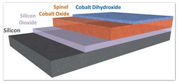
Schematic of the multi-functional water splitting catalyst layer engineered using atomic layer deposition for integration with a high-efficiency silicon cell. (Image: Ian Sharp/Berkeley Lab)
The research comes out of the Joint Center for Artificial Photosynthesis (JCAP), a DOE Energy Innovation Hub established in 2010 to develop a cost-effective method of turning sunlight, water, and carbon dioxide into fuel. JCAP is led by the California Institute of Technology with Berkeley Lab as a major partner.
The goal of this study was to strike a careful balance between the contradictory needs for efficient energy conversion and chemically sensitive electronic components to develop a viable system of artificial photosynthesis to generate clean fuel.
Striking the right balance
“In order for an artificial photosystem to be viable, we need to be able to make it once, deploy it, and have it last for 20 or more years without repairing it,” said study principal investigator Ian Sharp, head of materials integration and interface science research at JCAP.
The problem is that the active chemical environments needed for artificial photosynthesis are damaging to the semiconductors used to capture solar energy and power the device.
“Good protection layers are dense and chemically inactive. That is completely at odds with the characteristics of an efficient catalyst, which helps to split water to store the energy of light in chemical bonds,” said Sharp, who is also a staff scientist at Berkeley Lab’s Chemical Sciences Division. “The most efficient catalysts tend to be permeable and easily transform from one phase to another. These types of materials would usually be considered poor choices for protecting electronic components.”
By engineering an atomically precise film so that it can support chemical reactions without damaging sensitive semiconductors, the researchers managed to satisfy contradictory needs for artificial photosystems.
“This gets into the key aspects of our work,” said study lead author Jinhui Yang, who conducted the work as a postdoctoral researcher at JCAP. “We set out to turn the catalyst into a protective coating that balances these competing properties.”
Doing double duty
The researchers knew they needed a catalyst that could not only support active and efficient chemical reactions, but one that could also provide a stable interface with the semiconductor, allow the charge generated by the absorption of light from the semiconductor to be efficiently transferred to the sites doing catalysis, and permit as much light as possible to pass through.
They turned to a manufacturing technique called plasma-enhanced atomic layer deposition, performed at the Molecular Foundry at Berkeley Lab. This type of thin-film deposition is used in the semiconductor industry to manufacture integrated circuits.
“This technique gave us the level of precision we needed to create the composite film,” said Yang. “We were able to engineer a very thin layer to protect the sensitive semiconductor, then atomically join another active layer to carry out the catalytic reactions, all in a single process.”
The first layer of the film consisted of a nanocrystalline form of cobalt oxide that provided a stable, physically robust interface with the light-absorbing semiconductor. The other layer was a chemically reactive material made of cobalt dihydroxide.
“The design of this composite coating was inspired by recent advances in the field that have revealed how water-splitting reactions occur, at the atomic scale, on materials. In this way, mechanistic insights guide how to make systems that have the functional properties we need,” said Sharp.
Using this configuration, the researchers could run photosystems continuously for three days—potentially longer—when such systems would normally fail in mere seconds.
“A major impact of this work is to demonstrate the value of designing catalysts for integration with semiconductors,” said Yang. “Using a combination of spectroscopic and electrochemical methods, we showed that these films can be made compact and continuous at the nanometer scale, thus minimizing parasitic light absorption when integrated on top of photoactive semiconductors.”
The study authors noted that while this is an important milestone, there are many more steps needed before a commercially viable artificial photosystem is ready for deployment.
“In general, we need to know more about how these systems fail so we can identify areas to target for future improvement,” said Sharp. “Understanding degradation is an important avenue to making something that is stable for decades.”
Share on:


Suggested Items
Designer’s Notebook: What Designers Need to Know About Manufacturing, Part 2
04/24/2024 | Vern Solberg -- Column: Designer's NotebookThe printed circuit board (PCB) is the primary base element for providing the interconnect platform for mounting and electrically joining electronic components. When assessing PCB design complexity, first consider the component area and board area ratio. If the surface area for the component interface is restricted, it may justify adopting multilayer or multilayer sequential buildup (SBU) PCB fabrication to enable a more efficient sub-surface circuit interconnect.
Happy’s Tech Talk #27: Integrated Mesh Power System (IMPS) for PCBs
04/08/2024 | Happy Holden -- Column: Happy’s Tech TalkA significant decrease in HDI substrate production cost can be achieved by reducing the number of substrate layers from conventional through-hole multilayers and microvia multilayers of eight, 10, 12, and more to only two layers. Besides reducing direct processing steps, the yield will increase as defect-producing operations are eliminated. The integrated mesh power system (IMPS) was invented in the latter years of MCM-D use for thin-film fabrication. Those geometries fit today into our use of ultra HDI.
Insulectro’s 'Storekeepers' Extend Their Welcome to Technology Village at IPC APEX EXPO
04/03/2024 | InsulectroInsulectro, the largest distributor of materials for use in the manufacture of PCBs and printed electronics, welcomes attendees to its TECHNOLOGY VILLAGE during this year’s IPC APEX EXPO at the Anaheim Convention Center, April 9-11, 2024.
Now Available: Episode 4, Season 2 of Designing for Reality—Lamination
04/04/2024 | I-Connect007I-Connect007 has just released the latest episode of its podcast series, On the Line With..., which focuses on designing for reality in the electronics industry. Multilayer boards bring along a completely different set of processes. In this installment, ASC Sunstone VP/Manager Matt Stevenson discusses manufacturing techniques for multilayer boards. Of course, this necessitates a review of drill and registration techniques, followed by the ins and outs of lamination.
Heavy Copper PCBs: Bridging the Gap Between Design and Fabrication, Part 1
04/01/2024 | Yash Sutariya, Saturn Electronics ServicesThey call me Sparky. This is due to my talent for getting shocked by a variety of voltages and because I cannot seem to keep my hands out of power control cabinets. While I do not have the time to throw the knife switch to the off position, that doesn’t stop me from sticking screwdrivers into the fuse boxes. In all honesty, I’m lucky to be alive. Fortunately, I also have a talent for building high-voltage heavy copper circuit boards. Since this is where I spend most of my time, I can guide you through some potential design for manufacturability (DFM) hazards you may encounter with heavy copper design.