


 The Right Approach: I Hear the Train A Comin'
 It’s Only Common Sense: OCCAM—the Time Is Now
 Marcy's Musings: The Growing Industry
Artificial Control of Exciplexes Opens Possibilities for New Electronics
February 29, 2016 | Kyushu University, OPERAEstimated reading time: 3 minutes
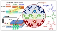
Demonstrating a strategy that could form the basis for a new class of electronic devices with uniquely tunable properties, researchers at Kyushu University were able to widely vary the emission color and efficiency of organic light-emitting diodes based on exciplexes simply by changing the distance between key molecules in the devices by a few nanometers.
This new way to control electrical properties by slightly changing the device thickness instead of the materials could lead to new kinds of organic electronic devices with switching behavior or light emission that reacts to external factors.
Organic electronic devices such as OLEDs and organic solar cells use thin films of organic molecules for the electrically active materials, making flexible and low-cost devices possible.
A key factor determining the properties of organic devices is the behavior of packets of electrical energy called excitons. An exciton consists of a negative electron attracted to a positive hole, which can be thought of as a missing electron.
In OLEDs, the energy in these excitons is released as light when the electron loses energy and fills the vacancy of the hole. Varying the exciton energy, for example, will change the emission color.
However, excitons are commonly localized on a single organic molecule and tightly bound with binding energies of about 0.5 eV. Thus, entirely new molecules must usually be designed and synthesized to obtain different properties from these Frenkel-type excitons, such as red, green, or blue emission for displays.
Researchers at Kyushu University's Center for Organic Photonics and Electronics Research (OPERA) instead focused on a different type of exciton called an exciplex, which is formed by a hole and electron located on two different molecules instead of the same molecule.
By manipulating the molecular distance between the electron-donating molecule (donor) and the electron-accepting molecule (acceptor) that carry the exciplex's hole and electron, respectively, the researchers could modify the properties of these weakly bound excitons.
"What we did is similar to placing sheets of paper between a magnet and a refrigerator," said Associate Professor Hajime Nakanotani, lead author of the paper reporting these results published online February 26, 2016, in the journal Science Advances.
"By increasing the thickness of an extremely thin layer of organic molecules inserted as a spacer between the donor and acceptor, we could reduce the attraction between the hole and electron in the exciplex and thereby greatly influence the exciplex's energy, lifetime, and emission color and efficiency."
Indeed, the changes can be large: by inserting a spacer layer with a thickness of only 5 nm between a donor layer and an acceptor layer in an OLED, the emission color shifted from orange to yellowish green and the light emission efficiency increased 700%.
For this to work, the organic molecule used for the spacer layer must have an excitation energy higher than those of the donor and acceptor, but such materials are already widely available.
While the molecular distance is currently determined by the thickness of the vacuum-deposited spacer layer, the researchers are now looking into other ways to control the distance.
"This gives us a powerful way to greatly vary device properties without redesigning or changing any of the materials," said Professor Chihaya Adachi, director of OPERA. "In the future, we envision new types of exciton-based devices that respond to external forces like pressure to control the distance and electrical behavior."
In addition, the researchers found that the exciplexes were still formed when the spacer was 10 nm thick, which is long on a molecular scale.
"This is some of the first evidence that electrons and holes could still interact like this across such a long distance," commented Professor Adachi, "so this structure may also be a useful tool for studying and understanding the physics of excitons to design better OLEDs and organic solar cells in the future."
"From both scientific and applications standpoints, we are excited to see where this new path for exciton engineering takes us and hope to establish a new category of exciton-based electronics."
Share on:


Suggested Items
Designer’s Notebook: What Designers Need to Know About Manufacturing, Part 2
04/24/2024 | Vern Solberg -- Column: Designer's NotebookThe printed circuit board (PCB) is the primary base element for providing the interconnect platform for mounting and electrically joining electronic components. When assessing PCB design complexity, first consider the component area and board area ratio. If the surface area for the component interface is restricted, it may justify adopting multilayer or multilayer sequential buildup (SBU) PCB fabrication to enable a more efficient sub-surface circuit interconnect.
Happy’s Tech Talk #27: Integrated Mesh Power System (IMPS) for PCBs
04/08/2024 | Happy Holden -- Column: Happy’s Tech TalkA significant decrease in HDI substrate production cost can be achieved by reducing the number of substrate layers from conventional through-hole multilayers and microvia multilayers of eight, 10, 12, and more to only two layers. Besides reducing direct processing steps, the yield will increase as defect-producing operations are eliminated. The integrated mesh power system (IMPS) was invented in the latter years of MCM-D use for thin-film fabrication. Those geometries fit today into our use of ultra HDI.
Insulectro’s 'Storekeepers' Extend Their Welcome to Technology Village at IPC APEX EXPO
04/03/2024 | InsulectroInsulectro, the largest distributor of materials for use in the manufacture of PCBs and printed electronics, welcomes attendees to its TECHNOLOGY VILLAGE during this year’s IPC APEX EXPO at the Anaheim Convention Center, April 9-11, 2024.
Now Available: Episode 4, Season 2 of Designing for Reality—Lamination
04/04/2024 | I-Connect007I-Connect007 has just released the latest episode of its podcast series, On the Line With..., which focuses on designing for reality in the electronics industry. Multilayer boards bring along a completely different set of processes. In this installment, ASC Sunstone VP/Manager Matt Stevenson discusses manufacturing techniques for multilayer boards. Of course, this necessitates a review of drill and registration techniques, followed by the ins and outs of lamination.
Heavy Copper PCBs: Bridging the Gap Between Design and Fabrication, Part 1
04/01/2024 | Yash Sutariya, Saturn Electronics ServicesThey call me Sparky. This is due to my talent for getting shocked by a variety of voltages and because I cannot seem to keep my hands out of power control cabinets. While I do not have the time to throw the knife switch to the off position, that doesn’t stop me from sticking screwdrivers into the fuse boxes. In all honesty, I’m lucky to be alive. Fortunately, I also have a talent for building high-voltage heavy copper circuit boards. Since this is where I spend most of my time, I can guide you through some potential design for manufacturability (DFM) hazards you may encounter with heavy copper design.