


 It’s Only Common Sense: Nice Guys Really Can Finish First
 The Right Approach: I Hear the Train A Comin'
 Marcy's Musings: The Growing Industry
Quantum Drag
July 21, 2016 | Iowa State UniversityEstimated reading time: 3 minutes
Friction and drag are commonplace in nature. You experience these phenomena when riding in an airplane, pairing electrical wiring, or rubbing pieces of sandpaper together.
Friction and drag also exist at the quantum level, the realm of atoms and molecules invisible to the naked eye. But how these forces interact across materials and energy sources remain in doubt.
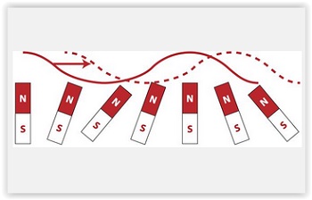
In a new study, University of Iowa theoretical physicist Michael Flatté proposes that a magnetic current flowing through a magnetic iron sheet will cause a current in a second, nearby magnetic iron sheet, even though the sheets aren't connected. The movement is created, Flatté and his team say, when electrons whose magnetic spin is disturbed by the current on the first sheet exert a force, through electromagnetic radiation, to create magnetic spin in the second sheet.
The findings may prove beneficial in the emerging field of spintronics, which seeks to channel the energy from spin waves generated by electrons to create smaller, more energy-efficient computers and electronic devices.
"It means there are more ways to manipulate through magnetic currents than we thought, and that's a good thing," says Flatté, senior author and team leader on the paper published June 9 in the journal Physical Review Letters.
Flatté has been studying how currents in magnetic materials might be used to build electronic circuits at the nanoscale, where dimensions are measured in billionths of a meter, or roughly 1/50,000 the width of a human hair. Scientists knew that an electrical current introduced in a wire will drag a current in another nearby wire. Flatté's team reasoned that the same effects may hold true for magnetic currents in magnetic layers.
In a magnetic substance, such as iron, each atom acts as a small, individual magnet. These atomic magnets tend to point in the same direction, like an array of tiny compasses fixated on a common magnetic point. But the slightest disturbance to the direction of just one of these atomic magnets throws the entire group into disarray: The collective magnetic strength in the group decreases. The smallest individual disturbance is called a magnon.
Flatté and his team report that a steady magnon current introduced into one iron magnetic layer will produce a magnon current in a second layer -- in the same plane of the layer but at an angle to the introduced current. They propose that the electron spins disturbed in the layer where the current was introduced engage in a sort of "cross talk" with spins in the other layer, exerting a force that drags the spins along for the ride.
"What's exciting is you get this response (in the layer with no introduced current), even though there's no physical connection between the layers," says Flatté, professor in the physics department and director of the Optical Science and Technology Center at the UI. "This is a physical reaction through electromagnetic radiation."
How electrons in one layer communicate and dictate action to electrons in a separate layer is somewhat bizarre.
Take electricity: When an electrical current flows in one wire, a mutual friction drags current in a nearby wire. At the quantum level, the physical dynamics appear to be different. Imagine that each electron in a solid has an internal bar magnet, a tiny compass of sorts. In a magnetic material, those internal bar magnets are aligned. When heat or a current is applied to the solid, the electrons' compasses get repositioned, creating a magnetic spin wave that ripples through the solid. In the theoretical case studied by Flatté, the disturbance to the solid excites magnons in one layer that then exert influence on the other layer, creating a spin wave in the other layer, even though it is physically separate.
"It turns out there is the same effect with spin waves," Flatté says.
Share on:


Suggested Items
Designer’s Notebook: What Designers Need to Know About Manufacturing, Part 2
04/24/2024 | Vern Solberg -- Column: Designer's NotebookThe printed circuit board (PCB) is the primary base element for providing the interconnect platform for mounting and electrically joining electronic components. When assessing PCB design complexity, first consider the component area and board area ratio. If the surface area for the component interface is restricted, it may justify adopting multilayer or multilayer sequential buildup (SBU) PCB fabrication to enable a more efficient sub-surface circuit interconnect.
Happy’s Tech Talk #27: Integrated Mesh Power System (IMPS) for PCBs
04/08/2024 | Happy Holden -- Column: Happy’s Tech TalkA significant decrease in HDI substrate production cost can be achieved by reducing the number of substrate layers from conventional through-hole multilayers and microvia multilayers of eight, 10, 12, and more to only two layers. Besides reducing direct processing steps, the yield will increase as defect-producing operations are eliminated. The integrated mesh power system (IMPS) was invented in the latter years of MCM-D use for thin-film fabrication. Those geometries fit today into our use of ultra HDI.
Insulectro’s 'Storekeepers' Extend Their Welcome to Technology Village at IPC APEX EXPO
04/03/2024 | InsulectroInsulectro, the largest distributor of materials for use in the manufacture of PCBs and printed electronics, welcomes attendees to its TECHNOLOGY VILLAGE during this year’s IPC APEX EXPO at the Anaheim Convention Center, April 9-11, 2024.
Now Available: Episode 4, Season 2 of Designing for Reality—Lamination
04/04/2024 | I-Connect007I-Connect007 has just released the latest episode of its podcast series, On the Line With..., which focuses on designing for reality in the electronics industry. Multilayer boards bring along a completely different set of processes. In this installment, ASC Sunstone VP/Manager Matt Stevenson discusses manufacturing techniques for multilayer boards. Of course, this necessitates a review of drill and registration techniques, followed by the ins and outs of lamination.
Heavy Copper PCBs: Bridging the Gap Between Design and Fabrication, Part 1
04/01/2024 | Yash Sutariya, Saturn Electronics ServicesThey call me Sparky. This is due to my talent for getting shocked by a variety of voltages and because I cannot seem to keep my hands out of power control cabinets. While I do not have the time to throw the knife switch to the off position, that doesn’t stop me from sticking screwdrivers into the fuse boxes. In all honesty, I’m lucky to be alive. Fortunately, I also have a talent for building high-voltage heavy copper circuit boards. Since this is where I spend most of my time, I can guide you through some potential design for manufacturability (DFM) hazards you may encounter with heavy copper design.