


 The Right Approach: I Hear the Train A Comin'
 It’s Only Common Sense: OCCAM—the Time Is Now
 Marcy's Musings: The Growing Industry
Perovskite PV: IDTechEx Discusses Resolving the Stability Challenge
July 26, 2022 | PRNewswireEstimated reading time: 2 minutes
Perovskite PV is an exciting new solar power technology. In 2009, the first report of a perovskite solar cell was published with an efficiency of just 3.9%. Just 10 years later, the record efficiencies surpassed 25% - comparable to conventional silicon technology following decades of research. Given the novelty of the technology, the rapid gains in efficiency are impressive; however, high efficiency is not the only promising attribute. Perovskite solar modules are significantly lighter than conventional silicon modules and can even be fabricated on flexible lightweight substrates. Versatility in module design makes them well-suited to a wide range of emerging applications such as self-powered electronics and Internet of Things devices. The new report published by IDTechEx, "Perovskite Photovoltaics 2023-2033", explores the commercialization potential of perovskite PV and identify the challenges remaining.
What is perovskite PV?
Perovskites refer to a family of materials with a specific material structure. The class of perovskites used in photovoltaics (PV) have a unique combination of electronic and optical properties that make it extremely well-suited to PV technology. Perovskite PV can provide similarly high-power density as silicon PV at lower cost, a fraction of the weight, and with a simpler manufacturing process. It can also be combined with silicon to create tandem cell architectures that can surpass the efficiency limits of single junction solar cells.
Efficiency gains dampened by stability concerns
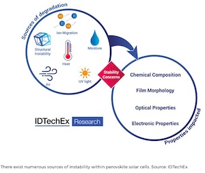
Despite the demonstration of high-efficiency perovskite modules, commercial adoption has been inhibited by concerns over long-term stability. Instability has a severely damaging effect on the electronic and optical properties of the module. There exist several sources of degradation that impact the stability and longevity of a perovskite module. These can be divided into two categories – intrinsic and extrinsic. Intrinsic instability is caused by defects and the migration of ions through the cell layers. Extrinsic instability is a result of contamination from the atmosphere, such as heat, moisture, oxygen, and UV radiation.
How can the stability challenge be resolved? There are two methods. The first is to encapsulate the cell to prevent the ingress of environmental elements. The transmittance rates of oxygen and water must be extremely low, and the encapsulant material must be optically transparent to visible light and ideally non-transparent to UV light. In the IDTechEx report, "Perovskite Photovoltaics 2023-2033", different conventional and emerging encapsulation methods are identified and benchmarked by their suitability. The second method involves tuning the perovskite's chemical composition to improve the resistance of the material. As the saying goes, nothing good comes for free. Modifying the chemical composition can improve the stability of the solar cell but may impact other properties such as efficiency and absorption spectrum. Encapsulation techniques and material engineering are crucial to preventing the degradation of the perovskite film. Solving these high-value problems is a compelling commercial opportunity.
Progress and Route to Commercialization
Resolving perovskite PV stability issues is challenging, with many strategies bringing performance trade-offs or extra costs. Nevertheless, the field has come a long way in its understanding of degradation mechanisms, and substantial progress has been made. Advancements in stabilizing perovskite solar cells have helped to transition the technology from academia to industry. Several companies, such as Oxford PV and Saule Technologies, are poised to enter the unestablished perovskite PV market within the next 2-3 years, with pilot studies and trials currently in progress.
Share on:


Suggested Items
Warm Windows and Streamlined Skin Patches – IDTechEx Explores Flexible and Printed Electronics
04/26/2024 | IDTechExFlexible and printed electronics can be integrated into cars and homes to create modern aesthetics that are beneficial and easy to use. From luminous car controls to food labels that communicate the quality of food, the uses of this technology are endless and can upgrade many areas of everyday life.
iNEMI Packaging Tech Topic Series: Role of EDA in Advanced Semiconductor Packaging
04/26/2024 | iNEMIAdvanced semiconductor packaging with heterogenous integration has made on-package integration of multiple chips a crucial part of finding alternatives to transistor scaling. Historically, EDA tools for front-end and back-end design have evolved separately; however, design complexity and the increased number of die-to-die or die-to-substrate interconnections has led to the need for EDA tools that can support integration of overall design planning, implementation, and system analysis in a single cockpit.
Koh Young Showcases Award-winning Inspection Solutions at SMTconnect with SmartRep in Hall 4A.225
04/25/2024 | Koh Young TechnologyKoh Young Technology, the industry leader in True 3D measurement-based inspection solutions, will showcase an array of award-winning inspection and measurement solutions at SMTconnect alongside its sales partner, SmartRep, in booth 4A.225 at NürnbergMesse from June 11-13, 2023. The following offers a glimpse into what Koh Young will present at the tradeshow:
Real Time with… IPC APEX EXPO 2024: Plasmatreat: Innovative Surface Preparation Solutions
04/25/2024 | Real Time with...IPC APEX EXPOIn this interview, Editor Nolan Johnson speaks with Hardev Grewal, CEO and president of Plasmatreat, a developer of atmospheric plasma solutions. Plasmatreat uses clean compressed air and electricity to create plasma, offering environmentally friendly methods for surface preparation. Their technology measures plasma density for process optimization and can remove organic micro-contamination. Nolan and Hardev also discuss REDOX-Tool, a new technology for removing metal oxides.
Nanotechnology Market to Surpass $53.51 Billion by 2031
04/25/2024 | PRNewswireSkyQuest projects that the nanotechnology market will attain a value of USD 53.51 billion by 2031, with a CAGR of 36.4% over the forecast period (2024-2031).