


 The Right Approach: I Hear the Train A Comin'
 It’s Only Common Sense: OCCAM—the Time Is Now
 Marcy's Musings: The Growing Industry
Can Electronics Manufacturing Join the Digital Age, Asks IDTechEx
March 29, 2023 | PRNewswireEstimated reading time: 3 minutes
Asked whether electronics is a 'digital technology', almost everyone would reply in the affirmative. However, while printed circuit boards (PCBs) enable digital technologies, the manufacturing processes used to produce them are still largely analog.
'Digital manufacturing' refers to any method that is directly controlled by a computer – simply using software in the design process doesn't count. Well-known examples are CNC (computer numerical control) machining, a subtractive method in which a rotational cutting tool selectively removes material, and 3D printing, an additive method that involves selective deposition of metal, plastic, or even ceramic. In both cases, direct computer control means that every part produced can have a different design and even that the design can be adjusted once manufacturing is in progress.
In contrast, conventional PCB manufacturing takes an analog approach. The desired pattern is transferred to a mask that is used for photolithography. Regions of material, typically copper laminate on a PCB, that are not coated with the patterned resist are then removed with an etchant. While this approach enables efficient high-yield production, introducing digital manufacturing methods would bring additional benefits.
Why Do We Need Digital Electronics Manufacturing?
Arguably, the main benefit of digital over analog manufacturing is that every item can be different with no additional setup time or costs. This is why inkjet printers (digital) are used at home since only a single copy is typically needed, whereas offset printing (analog) is used for mass-produced newspapers. With electronics, digital manufacturing enables rapid prototyping, accelerating the design process. It facilitates mass customization, where every circuit has a different design if desired without dramatically increasing production costs. Furthermore, high-resolution digital manufacturing methods can be used in conjunction with conventional photolithography to repair any unwanted circuit breaks.
Digital Manufacturing Methods for Electronics
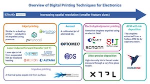
Interest in digital manufacturing methods for electronics has increased rapidly over recent years. While inkjet printing is by far the best-established method of digitally depositing conductive ink, there are a variety of emerging techniques that are both digital and additive. They all offer the direct control of digital manufacturing while spanning a range of throughputs, resolutions, material viscosity, and substrate dimensionality.
Print-then-plate utilizes inkjet printing of a thin layer of silver nanoparticle conductive ink to selectively pattern the substrate. This 'seed layer' is then fully metalized by electroless plating, producing a copper circuit. This method is already used for mass production. It combines the customizability of digital manufacturing, the reduced waste of additive manufacturing, and the conductivity of copper metal (rather than printed conductive ink).
Laser induced forward transfer (LIFT) can be regarded as a hybrid of laser direct structuring (LDS) and inkjet printing. Briefly, a laser heats conductive ink coated underneath a 'transfer plate', with evaporating solvent ejecting the ink. The lack of nozzle is a major benefit since it enables viscous inks typically used for screen printing to be used. There is potential for LIFT to be used in tandem with R2R production, enabling rapid, cost-effective production of customized circuits.
Aerosol printing is a relatively established technique that is well suited to printing onto 3D surfaces. A low-viscosity ink is atomized and formed into a thin collimated jet within a gas sheath layer, enabling resolutions as fine as 10 um with a working distance of up to 5cm. It's already being used in the semiconductor packaging production process and will soon be applied to larger area conformal surfaces such as automotive glass.
Electrohydrodynamic printing (EHD) uses an electric field to 'pull' ink from a nozzle rather than relying on pressure to 'push' out the ink. Capable of traces as narrow as 1um, this technique is currently being used to repair defects in TFT backplanes. An emerging approach is to combine hundreds of individually addressable nozzles within a single MEMS (micro electromechanical system) chip promises to break the resolution/throughput trade-off for small-scale additive electronics manufacturing.
Impulse printing is an innovative technique in the early stages of development that promises high throughput printing onto 3D surfaces, such as the edges of glass backplanes or 2.5D semiconductor packaging. The approach utilizes a rapid heat pulse from a controllable array of heating elements to expel ink from a flat 'transfer surface' onto the target object. Since no nozzle is used, ink can simultaneously be expelled from across the heated 'transfer surface'.
Share on:


Suggested Items
Warm Windows and Streamlined Skin Patches – IDTechEx Explores Flexible and Printed Electronics
04/26/2024 | IDTechExFlexible and printed electronics can be integrated into cars and homes to create modern aesthetics that are beneficial and easy to use. From luminous car controls to food labels that communicate the quality of food, the uses of this technology are endless and can upgrade many areas of everyday life.
Book Excerpt: The Printed Circuit Assembler’s Guide to... Factory Analytics
04/24/2024 | I-Connect007 Editorial TeamIn our fast-changing, deeply competitive, and margin-tight industry, factory analytics can be the key to unlocking untapped improvements to guarantee a thriving business. On top of that, electronics manufacturers are facing a tremendous burden to do more with less. If you don't already have a copy of this book, what follows is an excerpt from the introduction chapter of 'The Printed Circuit Assembler’s Guide to... Factory Analytics: Unlocking Efficiency Through Data Insights' to whet your appetite.
Listen Up! The Intricacies of PCB Drilling Detailed in New Podcast Episode
04/25/2024 | I-Connect007In episode 5 of the podcast series, On the Line With: Designing for Reality, Nolan Johnson and Matt Stevenson continue down the manufacturing process, this time focusing on the post-lamination drilling process for PCBs. Matt and Nolan delve into the intricacies of the PCB drilling process, highlighting the importance of hole quality, drill parameters, and design optimization to ensure smooth manufacturing. The conversation covers topics such as drill bit sizes, aspect ratios, vias, challenges in drilling, and ways to enhance efficiency in the drilling department.
Elevating PCB Design Engineering With IPC Programs
04/24/2024 | Cory Blaylock, IPCIn a monumental stride for the electronics manufacturing industry, IPC has successfully championed the recognition of the PCB Design Engineer as an official occupation by the U.S. Department of Labor (DOL). This pivotal achievement not only underscores the critical role of PCB design engineers within the technology landscape, but also marks the beginning of a transformative journey toward nurturing a robust, skilled workforce ready to propel our industry into the future.
Winner of The Science Show Rakett 69 Receives Incap Scholarship
04/24/2024 | IncapThe winner of the Rakett 69 science show, Andri Türkson, who stood out as an electronics enthusiast, received a scholarship from Incap Estonia, along with an internship opportunity in Saaremaa.