


 The Right Approach: I Hear the Train A Comin'
 It’s Only Common Sense: OCCAM—the Time Is Now
 Marcy's Musings: The Growing Industry
Siemens Unveils Calibre DesignEnhancer for Calibre Correct-by-construction IC Layout Optimization
July 12, 2023 | SiemensEstimated reading time: 3 minutes
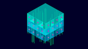
Siemens Digital Industries Software introduces Calibre DesignEnhancer software, an innovative solution that enables integrated circuit (IC), place-and-route (P&R) and full-custom design teams to dramatically improve productivity, boost design quality and reduce time to market by automatically implementing ‘Calibre correct-by-construction’ design layout modifications much earlier in the IC design and verification process.
The latest in a series of ‘shift left’ tools for Siemens’ industry-leading Calibre® nmPlatform for IC physical verification, the new Calibre DesignEnhancer tool empowers custom and digital design teams to enhance physical verification readiness by quickly and accurately optimizing their designs to reduce or eliminate voltage (IR) drop and electromigration (EM) issues. By supporting automated layout optimization during the IC design and implementation stages, the Calibre DesignEnhancer tool helps customers deliver “DRC-clean” designs to tapeout faster while improving design manufacturability and circuit reliability.
“The Calibre DesignEnhancer solution is proving to be extremely useful in our continuous efforts to enhance our IC design processes, for example, by addressing and resolving specification resistance and IR-drop issues,” said Pier Luigi Rolandi, Smart Power Technology R&D Design Enablement Director, STMicroelectronics.
Before conducting physical verification on an IC design, engineers have traditionally relied on third-party P&R tools to incorporate design for manufacturing (DFM) optimizations, often requiring multiple time-consuming runs before converging on a “DRC-clean” solution. With Siemens’ new Calibre DesignEnhancer tool, design teams can significantly shorten turnaround time and reduce EM/IR issues while preparing a layout for physical verification.
The Calibre DesignEnhancer tool currently provides three use models:
- Via modification automatically analyzes layouts and inserts up to 1 million+ Calibre-clean correct-by-construction vias to reduce the impact of via resistance on EM/IR and reliability. Because these modifications are based on a thorough understanding of the layout and signoff design rules, via insertion can help customers meet their power goals without impacting performance or area metrics.
- Power/ground enhancement automatically analyzes layouts and inserts Calibre nmDRC-clean vias and interconnects in open tracks to create parallel runs that can lower resistance on power/ground structures and reduce IR and EM issues associated with the power grid. Customers using the Calibre DesignEnhancer tool have achieved up to 90 percent reductions in IR drop issues.
- Filler cell insertion optimizes the insertion of decoupling capacitor (DCAP) and filler cells required for physical verification readiness. It replaces traditional P&R filler cell insertion processes, which helps to provide better quality of results and up to 10X faster runtimes.
“In today’s challenging IC design environment, engineering teams working at advanced nodes are struggling to optimize layouts for manufacturability and performance within the given area and project timeline constraints in which they must work,” said Michael White, Senior Director, Physical Verification Product Management, Calibre Design Solutions, Siemens Digital Industries Software. “By using the Calibre DesignEnhancer software, designers can bring Calibre polygonal processing speed and accuracy into play earlier in the design cycle, which can help to avoid late design cycle surprises.”
The Calibre DesignEnhancer solution uses proven technology, engines, and qualified rule decks from Calibre, all of which can help customers generate results that are correct by construction, Calibre DRC-clean, and ready for signoff verification. It can read OASIS, GDS, and LEF/DEF as input files, and output layout modifications in any combination of OASIS, GDS, or incremental DEF files, helping design teams to easily back-annotate Calibre DesignEnhancer software changes to the design database for power and timing analysis using commonly preferred tools for further analysis earlier in the design creation lifecycle.
The Calibre DesignEnhancer tool integrates with all major design and implementation environments using industry interface standards, providing a user-friendly environment that requires minimal training and setup. Calibre DesignEnhancer kits are available now for all leading foundries supporting designs from 130nm to 2nm, depending on the use model and the technology.
Share on:


Suggested Items
iNEMI Packaging Tech Topic Series: Role of EDA in Advanced Semiconductor Packaging
04/26/2024 | iNEMIAdvanced semiconductor packaging with heterogenous integration has made on-package integration of multiple chips a crucial part of finding alternatives to transistor scaling. Historically, EDA tools for front-end and back-end design have evolved separately; however, design complexity and the increased number of die-to-die or die-to-substrate interconnections has led to the need for EDA tools that can support integration of overall design planning, implementation, and system analysis in a single cockpit.
Cadence, TSMC Collaborate on Wide-Ranging Innovations to Transform System and Semiconductor Design
04/25/2024 | Cadence Design SystemsCadence Design Systems, Inc. and TSMC have extended their longstanding collaboration by announcing a broad range of innovative technology advancements to accelerate design, including developments ranging from 3D-IC and advanced process nodes to design IP and photonics.
Ansys, TSMC Enable a Multiphysics Platform for Optics and Photonics, Addressing Needs of AI, HPC Silicon Systems
04/25/2024 | PRNewswireAnsys announced a collaboration with TSMC on multiphysics software for TSMC's Compact Universal Photonic Engines (COUPE). COUPE is a cutting-edge Silicon Photonics (SiPh) integration system and Co-Packaged Optics platform that mitigates coupling loss while significantly accelerating chip-to-chip and machine-to-machine communication.
Siemens’ Breakthrough Veloce CS Transforms Emulation and Prototyping with Three Novel Products
04/24/2024 | Siemens Digital Industries SoftwareSiemens Digital Industries Software launched the Veloce™ CS hardware-assisted verification and validation system. In a first for the EDA (Electronic Design Automation) industry, Veloce CS incorporates hardware emulation, enterprise prototyping and software prototyping and is built on two highly advanced integrated circuits (ICs) – Siemens’ new, purpose-built Crystal accelerator chip for emulation and the AMD Versal™ Premium VP1902 FPGA adaptive SoC (System-on-a-chip) for enterprise and software prototyping.
Listen Up! The Intricacies of PCB Drilling Detailed in New Podcast Episode
04/25/2024 | I-Connect007In episode 5 of the podcast series, On the Line With: Designing for Reality, Nolan Johnson and Matt Stevenson continue down the manufacturing process, this time focusing on the post-lamination drilling process for PCBs. Matt and Nolan delve into the intricacies of the PCB drilling process, highlighting the importance of hole quality, drill parameters, and design optimization to ensure smooth manufacturing. The conversation covers topics such as drill bit sizes, aspect ratios, vias, challenges in drilling, and ways to enhance efficiency in the drilling department.