


 The Right Approach: I Hear the Train A Comin'
 It’s Only Common Sense: OCCAM—the Time Is Now
 Marcy's Musings: The Growing Industry
Built From the Bottom Up, Nanoribbons Pave the Way to 'On–Off' States for Graphene
March 31, 2017 | ORNLEstimated reading time: 4 minutes
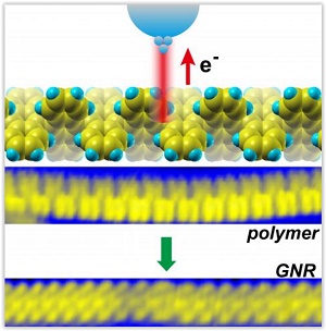
A new way to grow narrow ribbons of graphene, a lightweight and strong structure of single-atom-thick carbon atoms linked into hexagons, may address a shortcoming that has prevented the material from achieving its full potential in electronic applications. Graphene nanoribbons, mere billionths of a meter wide, exhibit different electronic properties than two-dimensional sheets of the material.
“Confinement changes graphene’s behavior,” said An-Ping Li, a physicist at the Department of Energy’s Oak Ridge National Laboratory. Graphene in sheets is an excellent electrical conductor, but narrowing graphene can turn the material into a semiconductor if the ribbons are made with a specific edge shape.
Previous efforts to make graphene nanoribbons employed a metal substrate that hindered the ribbons’ useful electronic properties.
Now, scientists at ORNL and North Carolina State University report in the journal Nature Communications that they are the first to grow graphene nanoribbons without a metal substrate. Instead, they injected charge carriers that promote a chemical reaction that converts a polymer precursor into a graphene nanoribbon. At selected sites, this new technique can create interfaces between materials with different electronic properties. Such interfaces are the basis of semiconductor electronic devices from integrated circuits and transistors to light-emitting diodes and solar cells.
“Graphene is wonderful, but it has limits,” said Li. “In wide sheets, it doesn’t have an energy gap—an energy range in a solid where no electronic states can exist. That means you cannot turn it on or off.”
When a voltage is applied to a sheet of graphene in a device, electrons flow freely as they do in metals, severely limiting graphene’s application in digital electronics.
“When graphene becomes very narrow, it creates an energy gap,” Li said. “The narrower the ribbon is, the wider is the energy gap.”
In very narrow graphene nanoribbons, with a width of a nanometer or even less, how structures terminate at the edge of the ribbon is important too. For example, cutting graphene along the side of a hexagon creates an edge that resembles an armchair; this material can act like a semiconductor. Excising triangles from graphene creates a zigzag edge—and a material with metallic behavior.
To grow graphene nanoribbons with controlled width and edge structure from polymer precursors, previous researchers had used a metal substrate to catalyze a chemical reaction. However, the metal substrate suppresses useful edge states and shrinks the desired band gap.
Li and colleagues set out to get rid of this troublesome metal substrate. At the Center for Nanophase Materials Sciences, a DOE Office of Science User Facility at ORNL, they used the tip of a scanning tunneling microscope to inject either negative charge carriers (electrons) or positive charge carriers (“holes”) to try to trigger the key chemical reaction. They discovered that only holes triggered it. They were subsequently able to make a ribbon that was only seven carbon atoms wide—less than one nanometer wide—with edges in the armchair conformation.
“We figured out the fundamental mechanism, that is, how charge injection can lower the reaction barrier to promote this chemical reaction,” Li said. Moving the tip along the polymer chain, the researchers could select where they triggered this reaction and convert one hexagon of the graphene lattice at a time.
Next, the researchers will make heterojunctions with different precursor molecules and explore functionalities. They are also eager to see how long electrons can travel in these ribbons before scattering, and will compare it with a graphene nanoribbon made another way and known to conduct electrons extremely well. Using electrons like photons could provide the basis for a new electronic device that could carry current with virtually no resistance, even at room temperature.
“It’s a way to tailor physical properties for energy applications,” Li said. “This is an excellent example of direct writing. You can direct the transformation process at the molecular or atomic level.” Plus, the process could be scaled up and automated.
Li conceived the project and designed the experiments. Chuanxu Ma, of ORNL, performed scanning tunneling microscopy with Li to characterize samples. Honghai Zhang and Kunlun Hong synthesized molecular precursors. Theoreticians Zhongcan Xiao and Jerry Bernholc (both of NCSU), Wenchang Lu (of ORNL and NCSU), and Jingsong Huang, Bobby Sumpter and Liangbo Liang (all three of ORNL) performed calculations that explained how charge injection lowers the barrier for the key chemical reaction.
The title of the current paper is “Controllable conversion of quasi-freestanding polymer chains to graphene nanoribbons.”
The Center for Nanophase Materials Sciences, a DOE Office of Science User Facility at ORNL, supported the work. Simulations at NCSU were supported by the DOE Office of Science. Supercomputing time was provided by the National Science Foundation at the National Center for Supercomputing Applications and by DOE through the Oak Ridge Leadership Computing Facility and the National Energy Research Scientific Computing Center, DOE Office of Science User Facilities at ORNL and Lawrence Berkeley National Laboratory, respectively. The Office of Naval Research funded electronic characterization of samples at CNMS and the corresponding calculations at NCSU. Oak Ridge Associated Universities supported Xiao’s work at CNMS. ORNL supported Liang’s Eugene P. Wigner Fellowship.
Share on:


Suggested Items
Warm Windows and Streamlined Skin Patches – IDTechEx Explores Flexible and Printed Electronics
04/26/2024 | IDTechExFlexible and printed electronics can be integrated into cars and homes to create modern aesthetics that are beneficial and easy to use. From luminous car controls to food labels that communicate the quality of food, the uses of this technology are endless and can upgrade many areas of everyday life.
Book Excerpt: The Printed Circuit Assembler’s Guide to... Factory Analytics
04/24/2024 | I-Connect007 Editorial TeamIn our fast-changing, deeply competitive, and margin-tight industry, factory analytics can be the key to unlocking untapped improvements to guarantee a thriving business. On top of that, electronics manufacturers are facing a tremendous burden to do more with less. If you don't already have a copy of this book, what follows is an excerpt from the introduction chapter of 'The Printed Circuit Assembler’s Guide to... Factory Analytics: Unlocking Efficiency Through Data Insights' to whet your appetite.
Listen Up! The Intricacies of PCB Drilling Detailed in New Podcast Episode
04/25/2024 | I-Connect007In episode 5 of the podcast series, On the Line With: Designing for Reality, Nolan Johnson and Matt Stevenson continue down the manufacturing process, this time focusing on the post-lamination drilling process for PCBs. Matt and Nolan delve into the intricacies of the PCB drilling process, highlighting the importance of hole quality, drill parameters, and design optimization to ensure smooth manufacturing. The conversation covers topics such as drill bit sizes, aspect ratios, vias, challenges in drilling, and ways to enhance efficiency in the drilling department.
Elevating PCB Design Engineering With IPC Programs
04/24/2024 | Cory Blaylock, IPCIn a monumental stride for the electronics manufacturing industry, IPC has successfully championed the recognition of the PCB Design Engineer as an official occupation by the U.S. Department of Labor (DOL). This pivotal achievement not only underscores the critical role of PCB design engineers within the technology landscape, but also marks the beginning of a transformative journey toward nurturing a robust, skilled workforce ready to propel our industry into the future.
Winner of The Science Show Rakett 69 Receives Incap Scholarship
04/24/2024 | IncapThe winner of the Rakett 69 science show, Andri Türkson, who stood out as an electronics enthusiast, received a scholarship from Incap Estonia, along with an internship opportunity in Saaremaa.