


 The Right Approach: I Hear the Train A Comin'
 It’s Only Common Sense: OCCAM—the Time Is Now
 Marcy's Musings: The Growing Industry
Baidu and Samsung Electronics Ready for Production of Leading-Edge AI Chip for Early Next Year
December 18, 2019 | SamsungEstimated reading time: 2 minutes
Baidu, a leading Chinese-language Internet search provider, and Samsung Electronics, a world leader in advanced semiconductor technology, today announced that Baidu’s first cloud-to-edge AI accelerator, Baidu KUNLUN, has completed its development and will be mass-produced early next year.
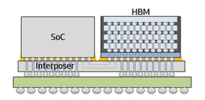
Baidu KUNLUN chip is built on the company’s advanced XPU, a home-grown neural processor architecture for cloud, edge, and AI, as well as Samsung’s 14-nanometer (nm) process technology with its I-Cube (Interposer-Cube) package solution.
The chip offers 512 gigabytes per second (GBps) memory bandwidth and supplies up to 260 Tera operations per second (TOPS) at 150 watts. In addition, the new chip allows Ernie, a pre-training model for natural language processing, to infer three times faster than the conventional GPU/FPGA-accelerating model.
Leveraging the chip’s limit-pushing computing power and power efficiency, Baidu can effectively support a wide variety of functions including large-scale AI workloads, such as search ranking, speech recognition, image processing, natural language processing, autonomous driving, and deep learning platforms like PaddlePaddle.
Through the first foundry cooperation between the two companies, Baidu will provide advanced AI platforms for maximizing AI performance, and Samsung will expand its foundry business into high performance computing (HPC) chips that are designed for cloud and edge computing.
“We are excited to lead the HPC industry together with Samsung Foundry,” said OuYang Jian, Distinguished Architect of Baidu. “Baidu KUNLUN is a very challenging project since it requires not only a high level of reliability and performance at the same time, but is also a compilation of the most advanced technologies in the semiconductor industry. Thanks to Samsung’s state of the art process technologies and competent foundry services, we were able to meet and surpass our goal to offer superior AI user experience. ”
“We are excited to start a new foundry service for Baidu using our 14nm process technology,” said Ryan Lee, vice president of Foundry Marketing at Samsung Electronics. “Baidu KUNLUN is an important milestone for Samsung Foundry as we’re expanding our business area beyond mobile to datacenter applications by developing and mass-producing AI chips. Samsung will provide comprehensive foundry solutions from design support to cutting-edge manufacturing technologies, such as 5LPE, 4LPE, as well as 2.5D packaging.”
As higher performance is required in diverse applications such as AI and HPC, chip integration technology is becoming more and more important. Samsung’s I-Cube technology, which connects a logic chip and high bandwidth memory (HBM) 2 with an interposer, provides higher density/ bandwidth on minimum size by utilizing Samsung’s differentiated solutions.
Compared to previous technology, these solutions maximize product performance with more than 50% improved power/signal integrity. It is anticipated that I-Cube technology will mark a new epoch in the heterogeneous computing market. Samsung is also developing more advanced packaging technologies, such as redistribution layers (RDL) interposer and 4x, 8x HBM integrated package.
Share on:


Suggested Items
Warm Windows and Streamlined Skin Patches – IDTechEx Explores Flexible and Printed Electronics
04/26/2024 | IDTechExFlexible and printed electronics can be integrated into cars and homes to create modern aesthetics that are beneficial and easy to use. From luminous car controls to food labels that communicate the quality of food, the uses of this technology are endless and can upgrade many areas of everyday life.
iNEMI Packaging Tech Topic Series: Role of EDA in Advanced Semiconductor Packaging
04/26/2024 | iNEMIAdvanced semiconductor packaging with heterogenous integration has made on-package integration of multiple chips a crucial part of finding alternatives to transistor scaling. Historically, EDA tools for front-end and back-end design have evolved separately; however, design complexity and the increased number of die-to-die or die-to-substrate interconnections has led to the need for EDA tools that can support integration of overall design planning, implementation, and system analysis in a single cockpit.
Koh Young Showcases Award-winning Inspection Solutions at SMTconnect with SmartRep in Hall 4A.225
04/25/2024 | Koh Young TechnologyKoh Young Technology, the industry leader in True 3D measurement-based inspection solutions, will showcase an array of award-winning inspection and measurement solutions at SMTconnect alongside its sales partner, SmartRep, in booth 4A.225 at NürnbergMesse from June 11-13, 2023. The following offers a glimpse into what Koh Young will present at the tradeshow:
Real Time with… IPC APEX EXPO 2024: Plasmatreat: Innovative Surface Preparation Solutions
04/25/2024 | Real Time with...IPC APEX EXPOIn this interview, Editor Nolan Johnson speaks with Hardev Grewal, CEO and president of Plasmatreat, a developer of atmospheric plasma solutions. Plasmatreat uses clean compressed air and electricity to create plasma, offering environmentally friendly methods for surface preparation. Their technology measures plasma density for process optimization and can remove organic micro-contamination. Nolan and Hardev also discuss REDOX-Tool, a new technology for removing metal oxides.
Nanotechnology Market to Surpass $53.51 Billion by 2031
04/25/2024 | PRNewswireSkyQuest projects that the nanotechnology market will attain a value of USD 53.51 billion by 2031, with a CAGR of 36.4% over the forecast period (2024-2031).