


 The Right Approach: I Hear the Train A Comin'
 It’s Only Common Sense: OCCAM—the Time Is Now
 Marcy's Musings: The Growing Industry
EV Group Establishes Heterogeneous Integration Competence Center
March 3, 2020 | PR NewswireEstimated reading time: 2 minutes
EV Group (EVG), a leading supplier of wafer bonding and lithography equipment for the MEMS, nanotechnology and semiconductor markets, announced that it has established the Heterogeneous Integration Competence Center™, which is designed to assist customers in leveraging EVG's process solutions and expertise to enable new and enhanced products and applications driven by advances in system integration and packaging. These include solutions and applications for high-performance computing and data centers, the Internet of Things (IoT), autonomous vehicles, medical and wearable devices, photonics and advanced sensors.
The Heterogeneous Integration Competence Center™ combines EV Group’s world-class wafer bonding, thin-wafer handling, and lithography products and expertise, as well as pilot-line production facilities and services at its state-of-the-art cleanroom facilities.
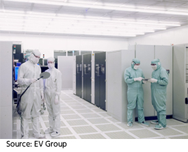
EVG’s HI Competence Center is designed to help enable new products and applications driven by advances in system integration and packaging. Shown here: chiplet integration by collective die-to-wafer hybrid bonding.
The Heterogeneous Integration (HI) Competence Center combines EVG's world-class wafer bonding, thin-wafer handling, and lithography products and expertise, as well as pilot-line production facilities and services at its state-of-the-art cleanroom facilities at EVG's headquarters in Austria, supported by EVG's worldwide network of process technology teams. Through the HI Competence Center, EVG will help customers to accelerate technology development, minimize risk, and develop differentiating technologies and products through heterogeneous integration and advanced packaging all while guaranteeing the highest IP protection standards that are required for working on pre-release products.
"Heterogeneous integration fuels new packaging architectures and demands new manufacturing technologies to support greater system and design flexibility, as well as increased performance and lower system design costs," stated Markus Wimplinger, corporate technology development & IP director of EV Group. "EVG's new HI Competence Center provides an open access innovation incubator for our customers and partners across the microelectronics supply chain to collaborate while pooling our solutions and process technology resources to shorten development cycles and time to market for innovative devices and applications enabled by heterogeneous integration."
EVG has an extensive background in heterogeneous integration, providing solutions for this key technology trend for more than 20 years. Among these are: permanent wafer bonding—including direct fusion and hybrid bonding for 3D packaging and metal bonding—and die-to-wafer bonding with and without collective carriers for integration of III-V compound semiconductors and silicon as well as high-density 3D packaging; temporary bonding and debonding, including mechanical, slide-off/lift-off, and UV laser assisted; thin-wafer handling; and innovative lithography technologies, including mask aligners, coaters and developers, and maskless exposure/digital lithography.
Advanced Packaging Milestones
In the field of permanent bonding, EVG pioneered the patented SmartView® wafer-to-wafer alignment system more than 20 years ago, and has refined this technology over the years to support breakthrough technology advances such as backside-illuminated CMOS image sensors (BSI-CIS) and more recently the first demonstration of sub-100-nm wafer-to-wafer alignment overlay for hybrid bonding—enabling devices such as 3D BSI-CIS and memory-on-logic stacking. EVG developed the first temporary bonding systems for ultra-thin wafers as early as 2001, which are essential for 3D/stacked die packaging, as well as revolutionized low-temperature laser debonding for ultra-thin and stacked fan-out packages.
In lithography, EVG cemented its position as a recognized technology leader with the delivery of the first UV molding solutions for high-volume production of wafer-level optics more than a decade ago, and has since led the proliferation of nanoimprint lithography (NIL) to high-volume manufacturing (HVM). EVG continues to break speed and accuracy barriers in mask alignment lithography for advanced packaging and, more recently, unveiled the world's first highly scalable maskless exposure technology, which addresses emerging requirements in HVM back-end lithography.
Share on:


Suggested Items
Koh Young Showcases Award-winning Inspection Solutions at SMTconnect with SmartRep in Hall 4A.225
04/25/2024 | Koh Young TechnologyKoh Young Technology, the industry leader in True 3D measurement-based inspection solutions, will showcase an array of award-winning inspection and measurement solutions at SMTconnect alongside its sales partner, SmartRep, in booth 4A.225 at NürnbergMesse from June 11-13, 2023. The following offers a glimpse into what Koh Young will present at the tradeshow:
Real Time with… IPC APEX EXPO 2024: Plasmatreat: Innovative Surface Preparation Solutions
04/25/2024 | Real Time with...IPC APEX EXPOIn this interview, Editor Nolan Johnson speaks with Hardev Grewal, CEO and president of Plasmatreat, a developer of atmospheric plasma solutions. Plasmatreat uses clean compressed air and electricity to create plasma, offering environmentally friendly methods for surface preparation. Their technology measures plasma density for process optimization and can remove organic micro-contamination. Nolan and Hardev also discuss REDOX-Tool, a new technology for removing metal oxides.
Nanotechnology Market to Surpass $53.51 Billion by 2031
04/25/2024 | PRNewswireSkyQuest projects that the nanotechnology market will attain a value of USD 53.51 billion by 2031, with a CAGR of 36.4% over the forecast period (2024-2031).
Cadence, TSMC Collaborate on Wide-Ranging Innovations to Transform System and Semiconductor Design
04/25/2024 | Cadence Design SystemsCadence Design Systems, Inc. and TSMC have extended their longstanding collaboration by announcing a broad range of innovative technology advancements to accelerate design, including developments ranging from 3D-IC and advanced process nodes to design IP and photonics.
SMC Korea 2024 to Highlight Semiconductor Materials Trends and Innovations on Industry’s Path to $1 Trillion
04/24/2024 | SEMIWith Korea a major consumer of semiconductor materials and advanced materials a key driver of innovation on the industry’s path to $1 trillion, industry leaders and experts will gather at SMC (Strategic Materials Conference) Korea 2024 on May 29 at the Suwon Convention Center in Gyeonggi-do, South Korea to provide insights into the latest materials developments and trends. Registration is open.