


 The Right Approach: I Hear the Train A Comin'
 It’s Only Common Sense: OCCAM—the Time Is Now
 Marcy's Musings: The Growing Industry
Darwin on a Chip
September 22, 2015 | MESA+ Institute for NanotechnologyEstimated reading time: 2 minutes
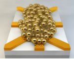
Researchers of the MESA+ Institute for Nanotechnology and the CTIT Institute for ICT Research at the University of Twente in The Netherlands have demonstrated working electronic circuits that have been produced in a radically new way, using methods that resemble Darwinian evolution. The size of these circuits is comparable to the size of their conventional counterparts, but they are much closer to natural networks like the human brain. The findings promise a new generation of powerful, energy-efficient electronics, and have been published in the leading British journal Nature Nanotechnology.
Learning from Nature
One of the greatest successes of the 20th century has been the development of digital computers. During the last decades these computers have become more and more powerful by integrating ever smaller components on silicon chips. However, it is becoming increasingly hard and extremely expensive to continue this miniaturisation. Current transistors consist of only a handful of atoms. It is a major challenge to produce chips in which the millions of transistors have the same characteristics, and thus to make the chips operate properly. Another drawback is that their energy consumption is reaching unacceptable levels. It is obvious that one has to look for alternative directions, and it is interesting to see what we can learn from nature. Natural evolution has led to powerful ‘computers’ like the human brain, which can solve complex problems in an energy-efficient way. Nature exploits complex networks that can execute many tasks in parallel.
Moving away from designed circuits
The approach of the researchers at the University of Twente is based on methods that resemble those found in Nature. They have used networks of gold nanoparticles for the execution of essential computational tasks. Contrary to conventional electronics, they have moved away from designed circuits. By using 'designless' systems, costly design mistakes are avoided. The computational power of their networks is enabled by applying artificial evolution. This evolution takes less than an hour, rather than millions of years. By applying electrical signals, one and the same network can be configured into 16 different logical gates. The evolutionary approach works around - or can even take advantage of - possible material defects that can be fatal in conventional electronics.
Powerful and energy-efficient
It is the first time that scientists have succeeded in this way in realizing robust electronics with dimensions that can compete with commercial technology. According to prof. Wilfred van der Wiel, the realized circuits currently still have limited computing power. “But with this research we have delivered proof of principle: demonstrated that our approach works in practice. By scaling up the system, real added value will be produced in the future. Take for example the efforts to recognize patterns, such as with face recognition. This is very difficult for a regular computer, while humans and possibly also our circuits can do this much better." Another important advantage may be that this type of circuitry uses much less energy, both in the production, and during use. The researchers anticipate a wide range of applications, for example in portable electronics and in the medical world.
Share on:


Suggested Items
Book Excerpt: The Printed Circuit Assembler’s Guide to... Factory Analytics
04/24/2024 | I-Connect007 Editorial TeamIn our fast-changing, deeply competitive, and margin-tight industry, factory analytics can be the key to unlocking untapped improvements to guarantee a thriving business. On top of that, electronics manufacturers are facing a tremendous burden to do more with less. If you don't already have a copy of this book, what follows is an excerpt from the introduction chapter of 'The Printed Circuit Assembler’s Guide to... Factory Analytics: Unlocking Efficiency Through Data Insights' to whet your appetite.
Listen Up! The Intricacies of PCB Drilling Detailed in New Podcast Episode
04/25/2024 | I-Connect007In episode 5 of the podcast series, On the Line With: Designing for Reality, Nolan Johnson and Matt Stevenson continue down the manufacturing process, this time focusing on the post-lamination drilling process for PCBs. Matt and Nolan delve into the intricacies of the PCB drilling process, highlighting the importance of hole quality, drill parameters, and design optimization to ensure smooth manufacturing. The conversation covers topics such as drill bit sizes, aspect ratios, vias, challenges in drilling, and ways to enhance efficiency in the drilling department.
Elevating PCB Design Engineering With IPC Programs
04/24/2024 | Cory Blaylock, IPCIn a monumental stride for the electronics manufacturing industry, IPC has successfully championed the recognition of the PCB Design Engineer as an official occupation by the U.S. Department of Labor (DOL). This pivotal achievement not only underscores the critical role of PCB design engineers within the technology landscape, but also marks the beginning of a transformative journey toward nurturing a robust, skilled workforce ready to propel our industry into the future.
Winner of The Science Show Rakett 69 Receives Incap Scholarship
04/24/2024 | IncapThe winner of the Rakett 69 science show, Andri Türkson, who stood out as an electronics enthusiast, received a scholarship from Incap Estonia, along with an internship opportunity in Saaremaa.
Alternative Manufacturing Inc. Awarded QML Requalification to IPC J-STD-001 and IPC-A-610
04/24/2024 | IPCIPC's Validation Services Program has awarded an IPC J-STD-001 and IPC-A-610 Qualified Manufacturers Listing (QML) requalification to Alternative Manufacturing Inc (AMI).