


 The Right Approach: I Hear the Train A Comin'
 It’s Only Common Sense: OCCAM—the Time Is Now
 Marcy's Musings: The Growing Industry
Imec and Ghent University Present Thermoplastically Deformable Electronic Circuits
October 28, 2015 | ImecEstimated reading time: 2 minutes
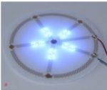
At this week’s Meeting of the International Microelectronics Assembly and Packaging Society (IMAPS 2015), imec and CMST (imec’s associated lab at Ghent University) present a novel technology for thermoplastically deformable electronics enabling low-cost 2.5D free-form rigid electronic objects. The technology is under evaluation in Philips LED lamp carriers, a downlight luminaire and a omnidirectional lightsource, to demonstrate the potential of this technology in innovative lighting applications.
Thanks to its energy-efficiency, excellent light quality, and high output power, light emitting diode (LED) technology is becoming the sustainable light source for the 21st century. But in addition, it also allows to design unprecedented, innovative lighting solutions. Imec and CMST’s new thermoplastically deformable electronic circuits now add a new dimension to the possibilities to fabricate novel lamp designs as well as smart applications in ambient intelligence and wearables.
The innovative technology is based on meander-shaped interconnects, a robust technique to realize dynamically stretchable elastic electronic circuits including LEDs. These are then embedded in thermoplastic polymers (e.g. polycarbonate). Following production on a flat substrate, using standard printed circuit board production equipment, the circuit is given its final form using thermoforming techniques such as vacuum forming, high pressure forming or even injection molding. Upon cooling, the thermoplastic retains its shape without inducing large internal stresses in the circuits. The method, based on standard available production processes, does not require large investments, reducing the cost of fabrication. The resulting designs have a low weight and low complexity, a high resilience, a low tooling and material cost, and a higher degree of manufacturer independence due to the standard industrial practices that are used.
The production process was developed in collaboration between the industrial and academic partners involved in the FP7 project TERASEL: imec, CMST (Ghent University), ACB, Holst Centre, Niebling Formtechnologie; Sintex NP and Philips Lighting BV. TERASEL is a European effort focusing on the development, industrial implementation and application of large-area, cost-effective, randomly shaped electronics and sensor circuit technologies.
About imec
Share on:


Suggested Items
Koh Young Showcases Award-winning Inspection Solutions at SMTconnect with SmartRep in Hall 4A.225
04/25/2024 | Koh Young TechnologyKoh Young Technology, the industry leader in True 3D measurement-based inspection solutions, will showcase an array of award-winning inspection and measurement solutions at SMTconnect alongside its sales partner, SmartRep, in booth 4A.225 at NürnbergMesse from June 11-13, 2023. The following offers a glimpse into what Koh Young will present at the tradeshow:
Real Time with… IPC APEX EXPO 2024: Plasmatreat: Innovative Surface Preparation Solutions
04/25/2024 | Real Time with...IPC APEX EXPOIn this interview, Editor Nolan Johnson speaks with Hardev Grewal, CEO and president of Plasmatreat, a developer of atmospheric plasma solutions. Plasmatreat uses clean compressed air and electricity to create plasma, offering environmentally friendly methods for surface preparation. Their technology measures plasma density for process optimization and can remove organic micro-contamination. Nolan and Hardev also discuss REDOX-Tool, a new technology for removing metal oxides.
Nanotechnology Market to Surpass $53.51 Billion by 2031
04/25/2024 | PRNewswireSkyQuest projects that the nanotechnology market will attain a value of USD 53.51 billion by 2031, with a CAGR of 36.4% over the forecast period (2024-2031).
Cadence, TSMC Collaborate on Wide-Ranging Innovations to Transform System and Semiconductor Design
04/25/2024 | Cadence Design SystemsCadence Design Systems, Inc. and TSMC have extended their longstanding collaboration by announcing a broad range of innovative technology advancements to accelerate design, including developments ranging from 3D-IC and advanced process nodes to design IP and photonics.
SMC Korea 2024 to Highlight Semiconductor Materials Trends and Innovations on Industry’s Path to $1 Trillion
04/24/2024 | SEMIWith Korea a major consumer of semiconductor materials and advanced materials a key driver of innovation on the industry’s path to $1 trillion, industry leaders and experts will gather at SMC (Strategic Materials Conference) Korea 2024 on May 29 at the Suwon Convention Center in Gyeonggi-do, South Korea to provide insights into the latest materials developments and trends. Registration is open.